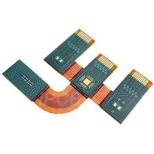
FPC PCBs Manufactured
FPC PCBs are one of the most crucial interconnection technologies in use for high-end electronics such as mobile phones, tablets, laptops and desktop computers. Their unique flexibility allows them to bend and flex, which can extend their lifespan and save space in an electronics product. They also offer greater heat dissipation than their rigid counterparts, which is a key feature in medical equipment and advanced military applications.
In order to deliver this functionality, however, these boards must be manufactured using specialized techniques designed for flexible substrates. This article provides an in-depth look at the end-to-end fabrication process that transforms raw materials into finished flexible circuits. Understanding the sequence of steps from material preparation through finish inspection can help designers optimize their designs for manufacturability and ensure that they stand up to dynamic mechanical environments.
The first step in the fpc pcb manufacturing process is to prepare the conductive materials and insulating materials. This is typically done by correcting or slitting the materials to accommodate various size requirements for final products. Once the materials are corrected or slit, they can then be pre-bonded with copper to create an FPC.
How Are FPC PCBs Manufactured?
Once the copper has been pre-bonded to the laminate, the next step is to apply the PCB design through photolithography technology. This step is usually performed on a flat surface, but can also be performed using a roll-to-roll lamination technique that utilizes RTR technology for optimal efficiency and cost savings.
During this step, the image is transferred from a positive mask to the copper using UV light. A negative mask is then applied to the conductive layer, which blocks the UV light from reaching areas of the circuit that shouldn’t be exposed, such as the pathways between components. The negative mask is then removed, revealing the copper pathways on the film. After the positive and negative image are etched, the copper is washed with an alkaline solution to remove any remaining photoresist. Once the wash is complete, the film is pressure-washed and allowed to dry.
Next, the coverlay on the FPC is fixed with a heat-curing epoxy. Afterwards, the PTH holes are created on the laminate with various drilling technologies. Laser drilling, body etching and chemical etching are common drilling methods used in the PCB industry. The hole walls are then prepared for the plating process that will connect layers on the FPC.
After the etching and plating processes are complete, the FPC is subjected to numerous tests that can evaluate the performance of the board in dynamic mechanical environments. These tests include resistance testing, insulation test and bending life testing. Once all of the tests are completed, the FPC is ready for shipment and assembly. This may involve the use of stiffeners to protect the circuits from flexing, or the attachment of silkscreen that guides assembly and identifies the board. Lastly, the board is subjected to an electrical test that confirms it functions properly. This step can be done by manual test or automated testing systems.